

没有合适的资源?快使用搜索试试~
我知道了~
MAX9296A DS.pdf
温馨提示
MAX9296A datasheet

General Description
The MAX9296A
deserializer converts single or dual serial
inputs to MIPI CSI-2 outputs. The device operates in either
GMSL1 or GMSL2 mode. The MAX9296A
also sends and
receives side-channel data, enabling full-duplex transmis
-
sion of forward path video and bidirectional control data
over
low-cost
50Ω
coax
or
100Ω
STPcables
to
meet
the
GMSL2 or GMSL1 channel specification.
The GMSL2 links operate at a fixed rate of 3Gbps or
6Gbps in the forward direction and 187.5Mbps in the
reverse direction. In GMSL1 mode, each serial link can
be paired with 3.12Gbps or 1.5Gbps GMSL1 serializ
-
ers or operate up to 4.5Gbps with GMSL2 serializers. The
MAX9296A
supports mixed GMSL2 and GMSL1 links.
The serial inputs operate independently
, allowing videos
with different timings and resolutions to be received on
each input.
Video data from both inputs can be aggregated for output
on a single CSI-2 port or replicated on a second port for
redundant processing.
Each four-lane CSI-2 port can be programmed to oper
-
ate with any number of active data lanes. Each CSI-2
port supports 16 virtual channels and allows virtual chan
-
nel and data type reassignment.
In GMSL1 and GMSL2 modes, the side-channel oper
-
ates at 9.6kbps to 1Mbps in UART
-to-UAR
T mode,
and 9.6kbps to 1Mbps in I
2
C-to-I
2
C mode with clock
stretching. Using the side-channel, a µC residing on
either end of the link can program serializer
, deserializer
,
and peripheral device registers independent of video tim
-
ing. In GMSL2 mode, two additional pass-through I
2
C or
UART
channels and a pass-through 50MHz SPI channel
provides peripheral control.
The MAX9296A
operates over the automotive tempera
-
ture range of -40°C to +105°C and is
AEC-Q100 qualified.
Applications
●
High-Definition (2MP+/4MP 60fps)
Advanced Driver
Assistance Systems (ADAS)
•
Surround View Systems (SVS)
•
Rear View Cameras (R
VC)
•
Camera Monitoring Systems (CMS)
•
Driver Monitoring Systems (DMS)
●
8MP 40fps Forward V
ision Cameras (FVC)
●
Satellite Lidar and Radar Sensors
●
Gesture Cameras
●
ECU-to-ECU Links
Ordering Information
appears at end of data sheet.
19-100424; Rev 0; 1
1/18
Benets and Features
●
Dual Four-Lane MIPI CSI-2 v1.3 Output Ports
•
Aggregation and Replication Functions
•
16-Channel Virtual Channel Support
•
Supports RA
W8/10/12/14/16/20, RGB565/666/888,
YUV4228-/10-bit,User-Dened,andGenericLong
Packet Data T
ypes
●
Advanced MIPI D-PHY v1.2
Transmitters
•
80Mbps to 2.0Gbps per Lane
•
Polarity Flip and Data-Lane Reassignment
●
Flexible Input Configuration
•
Independent Serial Inputs
Accept Video with
Different
Timing and Resolution
•
Support for Mixed GMSL2 and GMSL1 Inputs
●
Multiple GMSL2 Data Rates for System and Power
Flexibility
•
3Gbps or 6Gbps Forward Link Rates
•
187.5Mbps Reverse Link Rate
●
Backward-Compatible GMSL1 Mode
●
Full-Duplex Capability Over a Single Wire
●
Ideal for High-Definition Camera
Applications
•
Supports 2MP+/4MP at 60fps and 8MP
at 40fps
●
ASIL-Relevant Functional Safety Features (GMSL2)
•
ASIL-B Compliant in GMSL2 Mode
•
16-Bit CRC Protection of Side-Channel Data (I
2
C,
UART
, SPI, GPIO) with Retransmission Upon Error
Detection
•
Optional 32-Bit Video-Line CRC
•
Video W
atermark Insertion and Detection
●
Forward and Reverse Channel PRBS for BER
T
esting of Serial Link
●
Line Fault Monitoring
●
Continuous Link Margin Monitoring and Optimization
•
Adaptive Equalization
Allows 15m Coax Cable with
Multiple In-Line Connectors
•
Eye-Opening Monitor for Continuous Link Margin
Diagnosis
●
Concurrent Side-Channel for Device Configuration
and Communicating with Remote Peripherals
•
GMSL2: I
2
C/UART
, Pass-Through I
2
C/UART
, SPI,
GPIO and Register-Programmable GPIO
•
GMSL1: I
2
C/UART
, GPI-GPO Link and Register-
Programmable GPIO
•
Four Hardware-Programmable Device
Addresses
●
Compact 7mm x 7mm TQFN Package with Exposed Pad
Click
here
for production status of specic part numbers.
MAX9296A
Dual GMSL2/GMSL1 to CSI-2 Deserializer
EV
ALUA
TION
KIT A
V
AILABLE
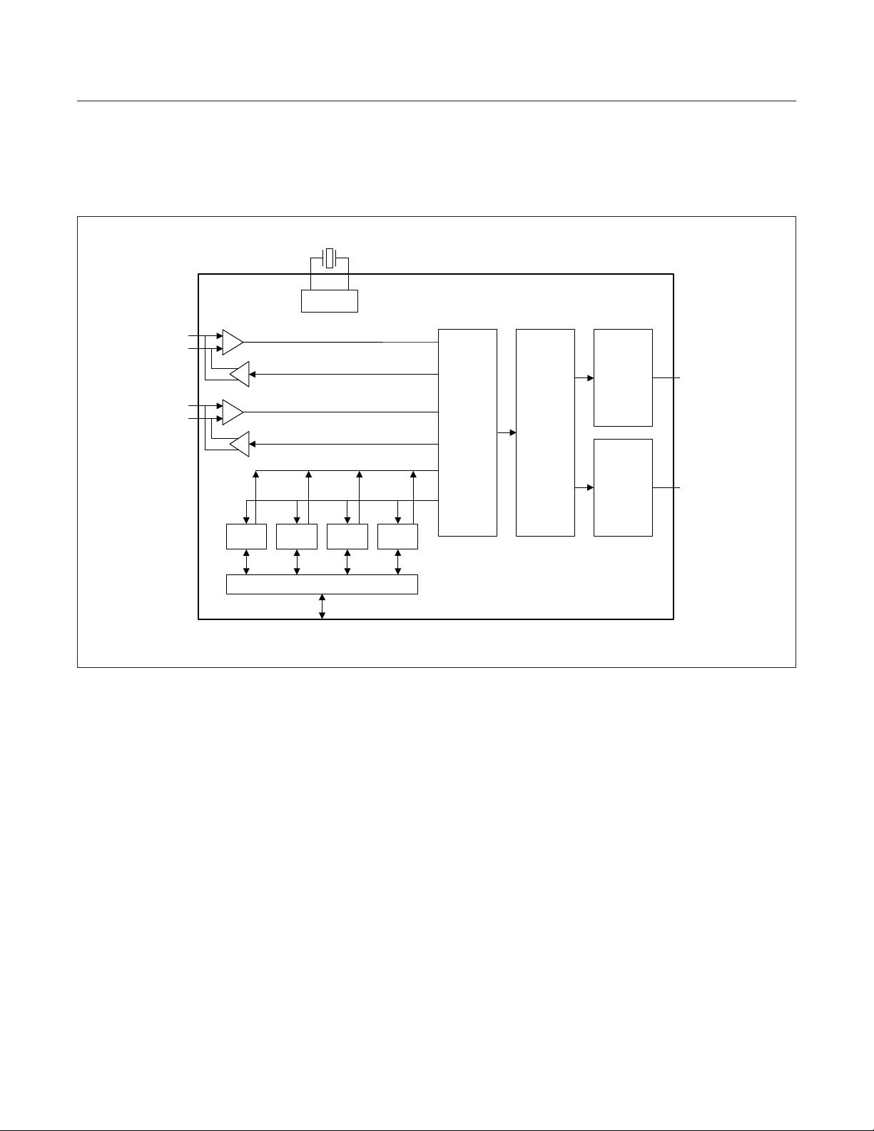
Simplied Block Diagram
GMSL2/
GMSL1
SERIAL
INTERFACE
SERIAL
INPUT
CH A
MAP TO MULTIFUNCTION I/O
I
2
C/
UART
SPI
GPIO
PLL
2x I
2
C
ROUTER
CSI-2
1 x 4
LANE
REVERSE CONTROL
FORWARD
CONTROL
CSI-2
1 x 4
LANE
SERIAL
INPUT
CH B
4-LANE
PORT A
4-LANE
PORT B
MULTIFUNCTION
www
.maximintegrated.com
Maxim Integrated
│
2
MAX9296A
Dual GMSL2/GMSL1 to CSI-2 Deserializer
Note A:
Active state means the device is powered up and not in sleep or power-down modes. Inactive means the device is not pow
-
ered up or powered up in sleep or power-down mode.
Note B:
Specified maximum voltage or 3.9V
, whichever is lower
.
Note C:
Specified maximum voltage or 1.36V
, whichever is lower
.
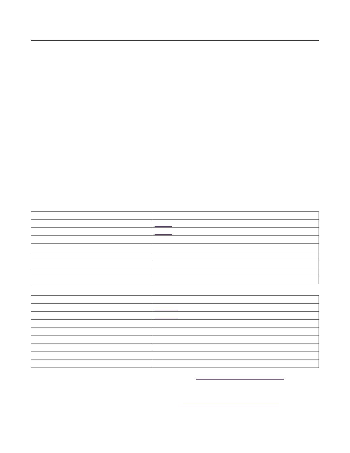
(All voltages with respect to ground.)
V
DDIO
...................................................................
-0.3V to +3.9V
V
DD18
...................................................................
-0.3V to +2.0V
V
DD
.......................................................................
-0.3V to +2.0V
V
TERM
................................................................
-0.3V to +1.32V
CAP_VDD.............................................................
-0.3V to +1.1V
SIO_ (Active State) (Note
A)
................
(V
DD18
- 1.1V) to V
DD18
SIO_ (Inactive state) (Note
A)
..............................
-0.3V to +1.1V
XRES, X2
..............................................
-0.3V to (V
DD18
+ 0.3V)
All Other Pins (Note B)
..........................
-0.3V to (V
DDIO
+ 0.3V)
DA/B_P/N, CKA/BP/N (Note C)
...........
-0.3V to (V
TERM
+ 0.1V)
Continuous Power Dissipation (T
A
= +70°C)
TQFN, TQFN-SW (Multilayer
,
derate 40mW/°C above +70°C)
...................................
2200
mW
TQFN, TQFN-SW (Single-layer
,
derate 27.8mW/°C above +70°C)
................................
1527mW
Storage T
emperature Range
............................
-40°C to +150°C
Soldering T
emperature (reflow)
.......................................
+260°C
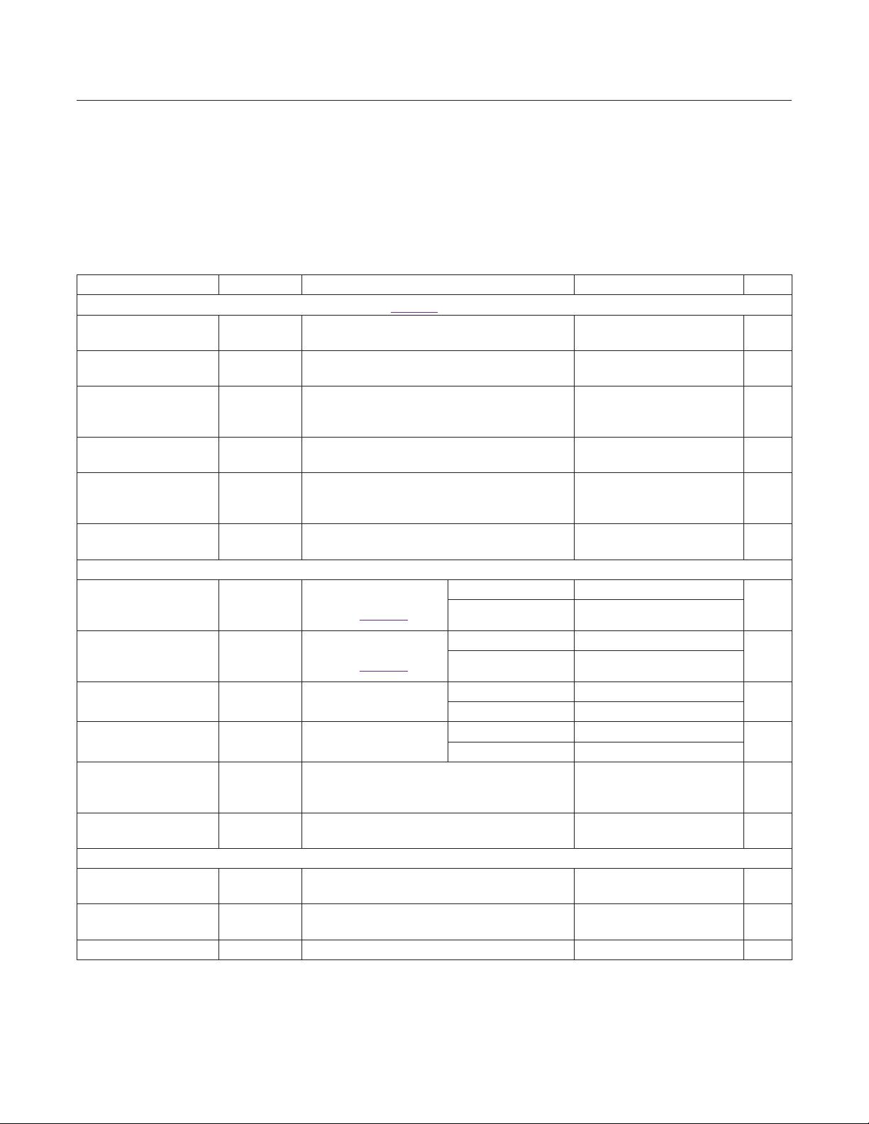
48-Pin TQFN
Package Code
T4877+1
1
Outline Number
21-0144
Land Pattern Number
90-0130
THERMAL RESIST
ANCE, SINGLE-LA
YER BOARD:
Junctionto
Ambient(θ
JA
)
36°C/W
JunctiontoCase(θ
JC
)
1°C/W
THERMAL RESIST
ANCE, FOUR-LA
YER BOARD:
Junctionto
Ambient(θ
JA
)
25°C/W
JunctiontoCase(θ
JC
)
1°C/W
48-Pin TQFN-SW (Side-Wettable)
Package Code
T4877Y+1
1
Outline Number
21-100045
Land Pattern Number
90-100016
THERMAL RESIST
ANCE, SINGLE-LA
YER BOARD:
Junctionto
Ambient(θ
JA
)
36°C/W
JunctiontoCase(θ
JC
)
1°C/W
THERMAL RESIST
ANCE, FOUR-LA
YER BOARD:
Junctionto
Ambient(θ
JA
)
25°C/W
JunctiontoCase(θ
JC
)
1°C/W
Absolute Maximum Ratings
Stresses
beyond
those
listed
under
“Absolute Maximum
Ratings”
may
cause
permanent
damage
to
the
device.
These
are
stress
ratings
only
,
and
functional
operation
of
the
device
at
these
or any
other conditions beyond
those indicated in
the operational sections
of the
specifications is not
implied. Exposure to
absolute maximum rating
conditions for
extended periods may
affect
device reliability
.
Package thermal resistances were obtained using the method described in JEDEC specification JESD51-7, using a four-layer board.
For detailed information on package thermal considerations, refer to
www
.maximintegrated.com/thermal-tutorial
.
For the latest package outline information and land patterns (footprints), go to
www
.maximintegrated.com/packages
. Note that a “+”,
“#”, or “-” in the package code indicates RoHS status only
. Package drawings may show a different suffix character
, but the drawing
pertains to the package regardless of RoHS status.
Package Information
www
.maximintegrated.com
Maxim Integrated
│
3
MAX9296A
Dual GMSL2/GMSL1 to CSI-2 Deserializer
(V
TERM
= 1.14V to 1.26V
, V
DD18
= 1.7V to 1.9V
, V
DD
= 0.95V to 1.05V or V
DD
= 1.14V to 1.26V
, V
DDIO
= 1.7V to 3.6V
, T
A
= -40°C
to +105°C, EP connected to PCB ground, typical values are at V
TERM
= 1.2V
, V
DD18
= V
DDIO
= 1.8V
, V
DD
= 1.0V
, T
A
= 25°C, unless
otherwise noted.) (Note 1)
P
ARAMETER
SYMBOL
CONDITIONS
MIN
TYP
MAX
UNITS
GMSL2 REVERSE CHANNEL SERIAL
OUTPUTS (S
ee
Figure
1
)
Output V
oltage Swing
(Single Ended)
V
O
R
L
=100Ω±1%
190
250
310
mV
Output V
oltage Swing
(Differential)
V
ODT
R
L
=100Ω±1%,peak-to-peakdifferential
voltage
380
500
620
mV
Change in V
OD
B
et
w
ee
n
Complementary
Output States
∆V
OD
R
L
=100Ω±1%,ΙV
OD(H)
-V
OD(L)
Ι
25
mV
Differential Output
Offset V
oltage
V
OS
R
L
=100Ω±1%,offsetvoltageineach
output state
V
DD18
- 0.45
V
DD18
-
0.3
V
DD18
-
0.15
V
Change in V
OS
B
et
w
ee
n
Complementary
Output S
ta
t
es
∆V
OS
R
L
=100Ω±1%,Ι(V
OS(H)
- V
OS(L)
)Ι
25
mV
T
ermination
Resistance (Internal)
R
T
Any pin to V
DD18
50
55
60
Ω
GMSL1 REVERSE CHANNEL SERIAL
OUTPUTS
Differential High Output
Peak V
oltage V
(SIO_P)
-
V
(SIO_N)
V
RODH
Forward channel
disabled (
Figure 2)
HIM disabled
30
70
mV
HIM enabled
50
11
0
Differential Low Output
Peak V
oltage V
(SIO_P)
-
V
(SIO_N)
V
RODL
Forward channel
disabled (
Figure 2)
HIM disabled
-70
-30
mV
HIM enabled
-1
10
-50
Single-Ended High
Output Peak V
oltage
V
ROSH
Forward channel
disabled
HIM disabled
30
70
mV
HIM enabled
50
11
0
Single-Ended Low
Output Peak V
oltage
V
ROSL
Forward channel
disabled
HIM disabled
-70
-30
mV
HIM enabled
-1
10
-50
Differential Output
Offset V
oltage
(V
(SIO_P)
+ V
(SIO_N)
)/2
V
DOS
V
DD18
-
0.3
V
DD18
V
T
ermination
Resistance (Internal)
R
T
Any pin to V
DD18
50
55
60
Ω
D-PHY LP
TRANSMITTER
Thevenin High-Level
Output V
oltage
V
OH
0.95
1.2
1.3
V
Thevenin Low-Level
Output V
oltage
V
OL
-50
50
mV
Output Impedance
Z
OLP
11
0
Ω
DC Electrical Characteristics
www
.maximintegrated.com
Maxim Integrated
│
4
MAX9296A
Dual GMSL2/GMSL1 to CSI-2 Deserializer
(V
TERM
= 1.14V to 1.26V
, V
DD18
= 1.7V to 1.9V
, V
DD
= 0.95V to 1.05V or V
DD
= 1.14V to 1.26V
, V
DDIO
= 1.7V to 3.6V
, T
A
= -40°C
to +105°C, EP connected to PCB ground, typical values are at V
TERM
= 1.2V
, V
DD18
= V
DDIO
= 1.8V
, V
DD
= 1.0V
, T
A
= 25°C, unless
otherwise noted.) (Note 1)
P
ARAMETER
SYMBOL
CONDITIONS
MIN
TYP
MAX
UNITS
D-PHY HS TRANSMITTER
HS T
ransmit
Static
Common-Mode V
oltage
V
CMTX
See
Figure 3
150
200
250
mV
V
CMTX
Mismatch When
Output Is Differential-1
Or Differential-0
|∆V
CMTX
(1,0)
|
∆V
CMTX(1,0)
= (V
CMTX(1)
- V
CMTX(0)
)/2,
(
Figure 4
)
5
mV
HS T
ransmit
Differential
V
oltage
|V
OD
|
See
Figure 3
140
200
270
mV
V
OD
Mismatch When
Output Is Differential-1
Or Differential-0
|∆V
OD
|
See
Figure 4
14
mV
HS Output High
V
oltage
V
OHHS
360
mV
Single-Ended Output
Impedance
Z
OS
40
50
62.5
Ω
Single-Ended Output
Impedance Mismatch
∆Z
OS
10
%
I/O PINS
High-Level Input
V
oltage
V
IH
0.7
x V
DDIO
V
Low-Level Input
V
oltage
V
IL
0.3
x V
DDIO
V
High-Level Output
V
oltage
V
OH
I
OH
= -4mA
V
DDIO
-
0.4
V
Low-Level Output
V
oltage
V
OL
I
OL
= 4mA
0.4
V
Input Current
I
IN
All pullup/pulldown devices disabled,
V
IN
= 0V to V
DDIO
1
μA
Input Capacitance
C
IN
3
pF
Internal Pullup/
Pulldown Resistance
R
IN
40kΩenabled
40
kΩ
1MΩenabled
1
MΩ
OPEN-DRAIN PINS
High-Level Input
V
oltage
V
IH
0.7
x V
DDIO
V
Low-Level Input
V
oltage
V
IL
0.3
x V
DDIO
V
Low-Level Open-Drain
Output V
oltage
V
OL
I
OL
= 4mA
0.4
V
DC
Electrical Characteristics (continued)
www
.maximintegrated.com
Maxim Integrated
│
5
MAX9296A
Dual GMSL2/GMSL1 to CSI-2 Deserializer
剩余297页未读, 继续阅读


评论3